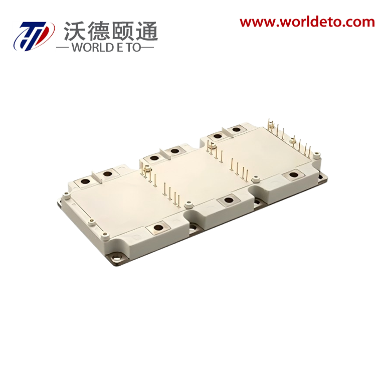
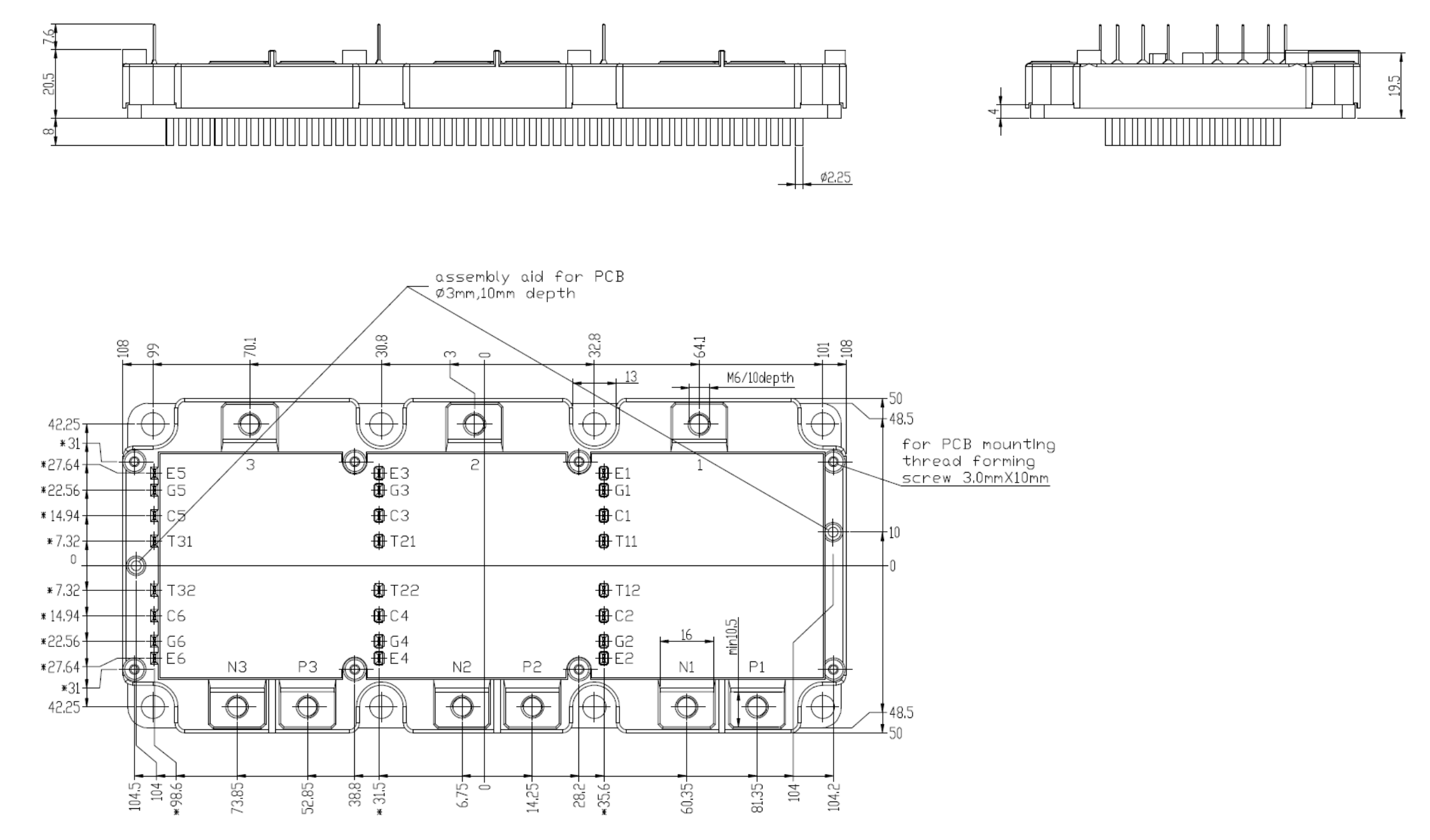
1200V400A Package:P4
Brief introduction
IGBT module,produced by STARPOWER. 1200V 400A.
Features
Typical Applications
Absolute Maximum Ratings TF=25oC unless otherwise noted
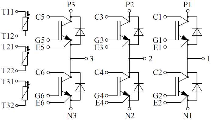
IGBT
Symbol |
Description |
Value |
Unit |
VCES |
Collector-Emitter Voltage |
1200 |
V |
VGES |
Gate-Emitter Voltage |
±20 |
V |
ICN |
Implemented Collector Current |
400 |
A |
IC |
Collector Current @ TF=25oC @ TF=75oC |
400 300 |
A |
ICM |
Pulsed Collector Current tp=1ms |
800 |
A |
PD |
Maximum Power Dissipation @ Tj=175oC |
1500 |
W |
Diode
Symbol |
Description |
Value |
Unit |
VRRM |
Repetitive Peak Reverse Voltage |
1200 |
V |
IFN |
Implemented Forward Current |
400 |
A |
IF |
Diode Continuous Forward Current |
300 |
A |
IFM |
Diode Maximum Forward Current tp=1ms |
800 |
A |
Module
Symbol |
Description |
Value |
Unit |
Tjmax |
Maximum Junction Temperature |
175 |
oC |
Tjop |
Operating Junction Temperature |
-40 to +150 |
oC |
TSTG |
Storage Temperature Range |
-40 to +125 |
oC |
VISO |
Isolation Voltage RMS,f=50Hz,t=1min |
2500 |
V |
IGBT Characteristics TF=25oC unless otherwise noted
Symbol |
Parameter |
Test Conditions |
Min. |
Typ. |
Max. |
Unit |
|
VCE(sat) |
Collector to Emitter Saturation Voltage |
IC=300A,VGE=15V, Tj=25oC |
|
1.50 |
1.95 |
V |
IC=300A,VGE=15V, Tj=125oC |
|
1.60 |
|
|||
IC=300A,VGE=15V, Tj=150oC |
|
1.65 |
|
|||
VGE(th) |
Gate-Emitter Threshold Voltage |
IC=16.0mA,VCE=VGE, Tj=25oC |
5.3 |
5.8 |
6.3 |
V |
ICES |
Collector Cut-Off Current |
VCE=VCES,VGE=0V, Tj=25oC |
|
|
1.0 |
mA |
IGES |
Gate-Emitter Leakage Current |
VGE=VGES,VCE=0V, Tj=25oC |
|
|
400 |
nA |
RGint |
Internal Gate Resistance |
|
|
0.5 |
|
Ω |
Cies |
Input Capacitance |
VCE=25V,f=1MHz, VGE=0V |
|
41.4 |
|
nF |
Cres |
Reverse Transfer Capacitance |
|
1.16 |
|
nF |
|
QG |
Gate Charge |
VGE=15V |
|
3.11 |
|
μC |
td(on) |
Turn-On Delay Time |
VCC=500V,IC=300A, RG=1.5Ω,VGE=±15V, Ls=25nH,Tj=25oC |
|
74 |
|
ns |
tr |
Rise Time |
|
31 |
|
ns |
|
td(off) |
Turn-Off Delay Time |
|
352 |
|
ns |
|
tf |
Fall Time |
|
255 |
|
ns |
|
Eon |
Turn-On Switching Loss |
|
4.01 |
|
mJ |
|
Eoff |
Turn-Off Switching Loss |
|
22.9 |
|
mJ |
|
td(on) |
Turn-On Delay Time |
VCC=500V,IC=300A, RG=1.5Ω,VGE=±15V, Ls=25nH,Tj=125oC |
|
81 |
|
ns |
tr |
Rise Time |
|
34 |
|
ns |
|
td(off) |
Turn-Off Delay Time |
|
411 |
|
ns |
|
tf |
Fall Time |
|
397 |
|
ns |
|
Eon |
Turn-On Switching Loss |
|
7.40 |
|
mJ |
|
Eoff |
Turn-Off Switching Loss |
|
32.2 |
|
mJ |
|
td(on) |
Turn-On Delay Time |
VCC=500V,IC=300A, RG=1.5Ω,VGE=±15V, Ls=25nH,Tj=150oC |
|
82 |
|
ns |
tr |
Rise Time |
|
36 |
|
ns |
|
td(off) |
Turn-Off Delay Time |
|
425 |
|
ns |
|
tf |
Fall Time |
|
434 |
|
ns |
|
Eon |
Turn-On Switching Loss |
|
8.90 |
|
mJ |
|
Eoff |
Turn-Off Switching Loss |
|
35.2 |
|
mJ |
|
|
ISC |
SC Data |
tP≤10μs,VGE=15V, Tj=150oC,VCC=900V, VCEM≤1200V |
|
1600 |
|
A |
Diode Characteristics TF=25oC unless otherwise noted
Symbol |
Parameter |
Test Conditions |
Min. |
Typ. |
Max. |
Unit |
|
VF |
Diode Forward Voltage |
IF=300A,VGE=0V,Tj=25oC |
|
1.70 |
2.15 |
V |
IF=300A,VGE=0V,Tj=125oC |
|
1.70 |
|
|||
IF=300A,VGE=0V,Tj=150oC |
|
1.70 |
|
|||
Qr |
Recovered Charge |
VR=500V,IF=300A, -di/dt=10600A/μs,VGE=-15V Ls=25nH,Tj=25oC |
|
15.0 |
|
μC |
IRM |
Peak Reverse Recovery Current |
|
391 |
|
A |
|
Erec |
Reverse Recovery Energy |
|
9.40 |
|
mJ |
|
Qr |
Recovered Charge |
VR=500V,IF=300A, -di/dt=9600A/μs,VGE=-15V Ls=25nH,Tj=125oC |
|
24.0 |
|
μC |
IRM |
Peak Reverse Recovery Current |
|
457 |
|
A |
|
Erec |
Reverse Recovery Energy |
|
18.4 |
|
mJ |
|
Qr |
Recovered Charge |
VR=500V,IF=300A, -di/dt=9500A/μs,VGE=-15V Ls=25nH,Tj=150oC |
|
29.0 |
|
μC |
IRM |
Peak Reverse Recovery Current |
|
488 |
|
A |
|
Erec |
Reverse Recovery Energy |
|
23.2 |
|
mJ |
NTC Characteristics TF=25oC unless otherwise noted
Symbol |
Parameter |
Test Conditions |
Min. |
Typ. |
Max. |
Unit |
R25 |
Rated Resistance |
|
|
5.0 |
|
kΩ |
∆R/R |
Deviation of R100 |
TC=100 oC,R100=493.3Ω |
-5 |
|
5 |
% |
P25 |
Power Dissipation |
|
|
|
20.0 |
mW |
B25/50 |
B-value |
R2=R25exp[B25/50(1/T2- 1/(298.15K))] |
|
3375 |
|
K |
B25/80 |
B-value |
R2=R25exp[B25/80(1/T2- 1/(298.15K))] |
|
3411 |
|
K |
B25/100 |
B-value |
R2=R25exp[B25/100(1/T2- 1/(298.15K))] |
|
3433 |
|
K |
Module Characteristics TF=25oC unless otherwise noted
Symbol |
Parameter |
Min. |
Typ. |
Max. |
Unit |
△p |
Pressure Drop Cooling Circuit △V/△t=10.0dm3/min;TF=25oC;Cooling Fluid=50% Water/50% Ethylene Glycol |
|
100 |
|
mbar |
p |
Maximum Pressure In Cooling Circuit |
|
|
2.5 |
bar |
LCE |
Stray Inductance |
|
14 |
|
nH |
RCC’+EE’ |
Module Lead Resistance, Terminal to Chip |
|
0.80 |
|
mΩ |
RthJF |
Junction-to-Cooling Fluid (perIGBT) Junction-to-Cooling Fluid (per Diode) |
|
|
0.100 0.125 |
K/W |
M |
Terminal Connection Torque, Screw M6 Mounting Torque, Screw M6 |
2.5 3.0 |
|
5.0 6.0 |
N.m |
G |
Weight of Module |
|
1250 |
|
g |
Our professional sales team are waiting for your consultation.
You can follow their product list and ask any questions you care about.